
Menu

Close
ADRF5473
Die on Carrier, Silicon Digital Attenuator, 0.5 dB LSB, 6-Bit, 100 MHz to 40 GHz


Overview
Features and Benefits
- Ultrawideband frequency range: 100 MHz to 40 GHz
- Attenuation range: 31.5 dB with 0.5 dB steps
- Bond pads for wire bond and ribbon bond
- Low insertion loss
- 1.7 dB typical up to 18 GHz
- 2.2 dB typical up to 26 GHz
- 3.2 dB typical up to 40 GHz
- Attenuation accuracy
- ±(0.10 + 2.0% of attenuation state) typical up to 26 GHz
- ±(0.13 + 1.5% of attenuation state) typical up to 35 GHz
- ±(0.30 + 1.5% of attenuation state) typical up to 40 GHz
- Typical step error
- ±0.12 dB typical up to 26 GHz
- ±0.30 dB typical up to 35 GHz
- ±0.60 dB typical up to 40 GHz
- High input linearity
- P0.1dB insertion loss state: 31 dBm typical
- P0.1dB other attenuation states: 28 dBm typical
- IP3: 50 dBm typical
- High RF power handling
- 26 dBm steady state average
- 31 dBm steady state peak
- Tight distribution in relative phase
- No low frequency spurious signals
- SPI and parallel mode control, CMOS/LVTTL compatible
- RF amplitude settling time (0.1 dB of final RF output): 250 ns
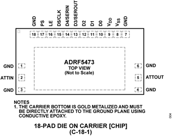
- 18-pad, 3.171 mm × 1.616 mm, die on carrier [CHIP]
Product Details
The ADRF5473 is a 6-bit digital attenuator with a 31.5 dB attenuation range in 0.5 dB steps manufactured in a silicon process attached on a gallium arsenide (GaAs) carrier substrate. The substrate incorporates the bond pads for chip and wire assembly, and the bottom of the device is metalized and connected to ground.
This device operates from 100 MHz to 40 GHz with better than 3.2 dB of insertion loss and excellent attenuation accuracy. The ADRF5473 has an RF input power handling capability of 26 dBm average and 31 dBm peak for all states.
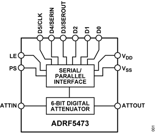
The ADRF5473 requires a dual-supply voltage of +3.3 V and −3.3 V. The device features serial peripheral interface (SPI), parallel mode control, and complementary metal-oxide semiconductor (CMOS)-/low voltage transistor to transistor logic (LVTTL)-compatible controls.
The ADRF5473 is designed to match a characteristic impedance of 50 Ω.
Note that when referring to a single function of a multifunction pad in the data sheet, only the portion of the pad name that is relevant is mentioned. For full pad names of the multifunction pads, refer to the section.
APPLICATIONS
Product Categories
Markets and Technologies
Product Lifecycle
 Recommended for New Designs
This product has been released to the market. The data sheet contains all final specifications and operating conditions. For new designs, ADI recommends utilization of these products.
Design Resources
ADI has always placed the highest emphasis on delivering products that meet the maximum levels of quality and reliability. We achieve this by incorporating quality and reliability checks in every scope of product and process design, and in the manufacturing process as well. "Zero defects" for shipped products is always our goal.


Support & Discussions
Sample & Buy
The USA list pricing shown is for BUDGETARY USE ONLY, shown in United States dollars (FOB USA per unit for the stated volume), and is subject to change. International prices may differ due to local duties, taxes, fees and exchange rates. For volume-specific price or delivery quotes, please contact your local Analog Devices, Inc. sales office or authorized distributor. Pricing displayed for Evaluation Boards and Kits is based on 1-piece pricing.